UIC chemical engineering researchers work on graphene-semiconductor’s ‘surface junction’ leads to emerging photovoltaics field
story title Heading link
University of Illinois Chicago researchers are hopeful their groundbreaking research with the thinnest possible material on the planet will have an immense impact on solar energy harvesting and help jumpstart a two-dimensional (2D) nanomaterial revolution in the field of photovoltaics.
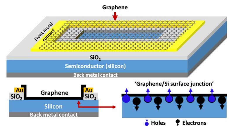
Sanjay Behura, research assistant professor with UIC’s Department of Chemical Engineering, Vikas Berry, head of the chemical engineering department, and colleagues published an article in Nature Photonics that reviewed their work on the surface junction in solar cells made with a 2D layer of graphene placed on top of a bulk three-dimensional (3D) semiconductor.
Berry said the paper discusses how ultrathin, 2D nanomaterials are helping to revolutionize photovoltaic systems that use light to create energy. In traditional systems, the junction, which is the boundary between two types of semiconductor materials, is buried beneath the surface and not easily accessible. But with the graphene-semiconductor, the layer of graphene on top is only one atom thick, so the junction is right below the surface.
This access allows researchers to manipulate or modify the junction, which is the driving force behind the energy created by a solar cell.
“We have already shown an 11-fold increase in plasmonic enhancement on graphene on silicon by adding silver nanoparticles on a graphene surface, which modifies the junction itself, since the junction is on the surface,” Berry said. “In conventional solar cells, the plasmonic particles have to be incorporated tediously in junctions buried under the surface to be effective.”
Being able to amplify the efficiency of solar cells is critical, as Behura noted traditional silicon-based solar cells appear to have hit their maximum efficiency levels. He added silicon solar cells are bulky and rigid, but newer cells that use 2D graphene can be lightweight and flexible. Graphene-on-semiconductor heterojunction is also a unique architecture as graphene plays the dual role of transparent electrode and photoactive absorber and charge-separating layer.
The 2D-graphene solar cells can also be integrated directly with circuits to create composite devices that are powered from within by 2D circuitry. Berry said one example of this kind of technology would be a wearable piece of clothing that has this technology built right into the product.
Another advantage to a graphene-on-3D-bulk semiconductor system is it can be built efficiently without the use of toxic elements, according to Behura. In contrast, the process to build traditional silicon solar cells is energy intensive and some can be environmentally unstable.
“It is not harmful and is environmentally safe, and would be a really good alternative energy source,” Berry said.
In addition to their specific work-on-graphene semiconductors, the researchers said the 2D nanomaterial on a 3D semiconductor architecture has opened the door for a whole new field of research using ultrathin materials.
Behura said tandem 2D junctions are also possible, where a solar cell would have two layers of different 2D nanomaterials on top of a 3D semiconductor. The ability to see and manipulate the junction in the solar cell will allow researchers to enhance the power conversion efficiency.
“The 2D/3D mixed-dimensional emerging photovoltaics is a complex system and therefore, requires further investigations on the surface science of 2D layers and interface engineering of 2D/3D junctions,” Behura said.
“The other reason why this is so exciting is now we have thousands of different 2D nanomaterials,” Berry said. “And we have thousands of semiconductors and we have thousands of things you can do with a solar cell. So effectively you can make millions and billions of different combinations of these devices. This will explode into a new field of its own.”
While Berry has expertise in graphene-based interfaces, Behura has studied the science of mixed-dimensional surface-based photo-junctions for a decade. They are both the lead authors of this paper, and the other authors Chen Wang and Yu Wen, graduate students in chemical and electrical engineering, respectively. The presented work was supported by the National Science Foundation, Office of Naval Research, and Dimerond Technologies.